Table Of Content
As you route your board, try to come up with a strategy to finish your important routes first, then fill in the gaps with the remaining connections as needed. Some of the important routes will include your power nets, any impedance-controlled nets, and any noise-sensitive nets like low-level analog signals. Be sure to utilize good routing guidelines and take advantage of Altium Designer tools to simplify the process, such as highlighting nets and interactive routing features. Wherever controlled electromagnetism exists, printed circuit boards form the infrastructure to maintain it. Of course, circuit boards don’t just spring out from nothingness–their design and manufacturing are a huge engineering undertaking unto themselves. Circuit boards are built with a dielectric core material with poor electrical conducting properties to ensure pure circuitry transmission and interspaced with extra layers of metal and dielectric as needed.
Source Data Extended Data Fig. 5
The dielectric and mechanical properties of the core and prepreg will determine reliability and signal/power integrity in the design, and they should be selected carefully when designing for high-reliability applications. For example, military and medical applications need highly reliable designs that might be deployed in harsh environments, and a PCB for a telecom system might require a low-loss PTFE laminate in a small package. Circuit designers, PCB layout engineers, and simulation engineers trust the complete set of circuit board design tools in Altium Designer®. When a circuit board design is finished and ready to be released to manufacturing, the Altium 365™ platform makes it easy to collaborate and share your projects. The functionality and capabilities discussed here only scratch the surface of what is available to you. To explore these and other options, try Altium Designer yourself with a free trial.
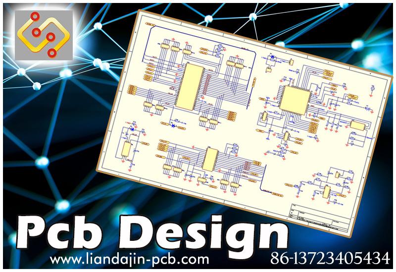
Schematic Design: The First Step in the PCB Design Process
If your PCB does have layers, the right way of trace routing is to exchange directions between layers. A great rule to follow in power outlets is to design with the star-configuration in mind, rather than daisy-chain your connections. If you daisy-chain, that means your connections are running from one component to another.
Source data
TTM Technologies, Inc.This Chippewa Falls, WI, company has a total of 887 employees. KiCad's 3D Viewer allows easy inspection of your PCB to check mechanical fit and to preview your finished product.A built-in raytracer with customizable lighting can create realistic images to show off your work. At EMSG Inc., we know that success in the electronics manufacturing industry depends on attention to detail at every level, from the beginning stages of planning to the shipment of the last part. That’s why we make it a priority to deliver to you exactly what it is you need to get the job done.
Step 3: Synchronize Schematics to Your PCB Board Design
Advanced PCB technologies, such as flexible, rigid-flex, and high-density interconnect (HDI) PCBs, have been developed to address the challenges of increasingly complex and compact electronic devices. Understanding the diverse types of printed circuit boards is instrumental in selecting the most suitable option for a particular application. A printed circuit board is a flat board made of non-conductive material, usually fiberglass, which gets etched with a network of copper traces connecting various electronic components.
High-Density Interconnect (HDI) PCBs
Circuit board parts have been traditionally difficult to find, and many designers have spent hours creating these parts manually. Altium Designer offers access to a Manufacturer Part Search panel, which helps you quickly add components to your library. All you have to do is search and click to download accurate parts directly from a managed library. At this point, the board is ready to be built, and the first step is to send the output data files to a facility for fabrication.
DuPont Showcases Industry-Leading Innovations in Advanced Circuit Materials and Solutions at TPCA Show 2023 in ... - DuPont
DuPont Showcases Industry-Leading Innovations in Advanced Circuit Materials and Solutions at TPCA Show 2023 in ....
Posted: Wed, 25 Oct 2023 07:00:00 GMT [source]
Addressing these challenges is essential for producing high-quality, reliable, and cost-effective PCBs. FR-4, a glass-reinforced epoxy laminate, is widely used in the PCB industry due to its balanced electrical, thermal, and mechanical properties. With a dielectric constant of 4.5 at 1 MHz and a dissipation factor of 0.02, FR-4 is suitable for general-purpose applications.
For example, a four-layer PCB may have a layer stackup consisting of a top signal layer, a ground plane, a power plane, and a bottom signal layer. This configuration establishes a stable foundation for signal transmission, reduces electromagnetic interference (EMI) disruptions, and facilitates effective power distribution. In more complex designs, additional layers may be added to accommodate higher component density, high-speed signals, or advanced features like embedded components or blind and buried vias. The layer stack up design is crucial for maintaining signal integrity and ensuring the proper functionality of PCB. A well-designed layer stackup considers factors such as signal return paths, impedance control, and crosstalk reduction.
Impedance matching and termination are critical techniques used in PCB design to maintain signal integrity and minimize signal reflections. When a signal encounters a change in impedance, such as when it transitions from a trace to a component or from one PCB layer to another, a portion of the signal energy is reflected back toward the source. These reflections can cause signal distortion, ringing, and other issues that degrade the quality of the signal. Poor signal integrity and EMC can lead to a variety of problems, including signal distortion, crosstalk, noise, and EMI.
Engage with fellow PCB designers, ask questions, and share your experiences to enhance your skills and troubleshoot any issues you may encounter. This swelled the vPCB's plastic without damaging the glass sheets and electronic components, letting the researchers extract these for reuse. A team led by researchers at the University of Washington developed a new PCB that performs on par with traditional materials and can be recycled repeatedly with negligible material loss. Researchers used a solvent that transforms a type of vitrimer—a cutting-edge class of sustainable polymers—to a jelly-like substance without damaging it, allowing the solid components to be plucked out for reuse or recycling.
Vias are small holes drilled through the PCB that provide electrical connections between different layers. Proper via placement can help minimize signal degradation and improve overall circuit performance. When creating a schematic, designers use a variety of standard symbols to represent different types of components.
For your PCB designing tutorial, Altium gives you access to on-demand webinars, design tutorials, and the AltiumLive forum. You’ll have the tools and resources you need for successful printed circuit board design in Altium Designer. Before you create your manufacturer deliverables, it’s always a good idea to verify your circuit board layout by running a design rule check (DRC). Altium Designer will do this automatically as you layout your components and route your circuit board design, but it never hurts to run another DRC manually.


No comments:
Post a Comment